Contact
DFM A/S
Kogle Allé 5
DK-2970 Hørsholm
Denmark
Tlf: +45 7730 5800
E-mail: [email protected]
CVR/VAT#: DK29217939
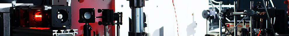
DFM has a range of state-of-the-art equipment
Below we list some of the equipment DFM has available for lease. In some cases, however, only when operated by DFM staff.
Please do not hesitate to contact us at [email protected] if you are interested in knowing more about lease of equipment.
Equipment list
| EQUIPMENT | DESCRIPTION |
| Atomic force microscope (AFM) | (Park System NX-20) |
| Measurement range 100 × 100 × 15 µm3. Calibrated with a measurement accuracy down to 0.02 % for periods of 1 µm and 1 nm for step heights of 20 nm | |
| Liquid cell and temperature control from 4°C to 180°C. | |
| Material properties measured by AFM indentation. Force from 0 to 1 mN with resolution down to 1 nN. Depth of indentation up to 1 µm with a resolution of 0.1 nm. Young’s modulus for the surface can be estimated in the range from 1 MPa to 10 GPa | |
| Scanning Kelvin Probe Force Microscopy (SKPFM) determines a DC potential difference between tip and sample which can be related to the work function of surface electrons: Dynamic range ±10 eV, noise level 0.02 eV | |
| Conductive atomic force microscopy measuring a current between AFM tip and a conductive sample which can be related to the local electronic properties such as the local density. | |
| AFM tips, more than 30 different types with radii of curvature from 2 nm to 0.75 µm and spring constant from 0.03 N/m to 2000 N/m. Available tip materials of e.g. silicon, tungsten carbide and diamond, polystyrene, gold, quartz and conductive tips with platinum from e.g. NanoSensors, TeamNanotech, etc. | |
| AFM | (Bruker Multimode 8) |
| Measurement volume up to 150 µm × 150 µm × 5 µm with a measurement uncertainty of 2 % to 10 % | |
| Liquid cell and temperature control 20°C to 60°C. | |
| Material properties measured by AFM indentation. Force from 0 to 1 mN with resolution down to 1 nN. Depth of indentation up to 1 µm with a resolution of 0.1 nm. | |
| Scanning Kelvin Probe Force Microscopy (SKPFM) determines a DC potential difference between tip and sample which can be related to the work function of surface electrons: Dynamic range ±10 eV, noise level 0.02 eV | |
| Conductive atomic force microscopy measuring a current between AFM tip and a conductive sample which can be related to the local electronic properties such as the local density. | |
| AFM tips, more than 30 different types with radii of curvature from 2 nm to 0.75 µm and spring constant from 0.03 N/m to 2000 N/m. Available tip materials of e.g. silicon, tungsten carbide and diamond, polystyrene, gold, quartz and conductive tips with platinum from e.g. NanoSensors, TeamNanotech, etc. | |
| Confocal and interference microscope | (Sensofar PLu Neox) |
| Non contact 3D profiling, confocal and interference microscope with six objectives, a lateral measurement range from 85 × 64 µm2 to 1.27 × 0.97 mm2, and a vertical measurement range from 5 nm to 10 mm. The instrument is calibrated with lateral measurement accuracy down to 0.15 % for a period of 10 µm and a vertical measurement accuracy down to 3 nm | |
| Surface topology. Fast and precise measurement of surfaces and interfaces protected by a transparent layer. | |
| Optical diffraction microscope | (Designed and developed by DFM) |
| Measurement of surface topologies with an accuracy down to 1 nm | |
| Real time surface profiling | |
| Diffraction setup | (Designed and developed by DFM) |
| Two rotational stages and goniometres with a relative accuracy better than 3 × 10⁻⁴. Measurement of grating periods with an accuracy better than 0.5 nm for gratings with a period larger than 1 µm | |
| Roughness measurement equipment: Calibration of optical instruments for surface roughness measurements. | |
| Mueller Polariometer | (Designed and developed by DFM) |
| Measurement of surface topology, thin films and refractive indices for materials. | |
| Refractive index for thin films with an absolute accuracy down to 1 × 10⁻³ | |
| The thickness of thin films with a relative accuracy down to 5 × 10⁻⁴ | |
| The line width of periodic structures with an absolute accuracy down to 0.5 nm | |
| The height of periodic structures with an absolute accuracy down to 1.0 nm | |
| Particle Counter Spectrometer | (Particle Measuring Systems LAS-X II) |
| 0.1 µm to 7 µm in 100 channels. | |
|
Measurement of particle number concentrations for airborne particles with an average diameter between 300 nm and 5000 nm. Typical measurement uncertainties on the particle number concentration is between 5% and 8% |
|
| Roughness profilometer | (Taylor Hobson) |
| Mesurement uncertainty about 2% for Ra = 6 µm | |
| Interferometer | (Zygo) |
| Displacement measurement. Calibrated with an accuracy down to 0.3 nm or 4 × 10⁻⁷ | |
| Stage | (nPoint) |
| Scanning range 500 µm × 500 µm (PI) and stage with a scanning range of 400 µm × 400 µm × 100 µm | |
| Dimensional Standards | Traceable to international recoqnised standards |
| Step height of nominal 1 µm with an uncertainty of 1.2 nm | |
| Two-dimensional grating with a period of 1 µm and an uncertainty of 0.017 nm | |
| Software | |
| Software package for nano- and microscale image processing and analysis (SPIP – Scanning Probe Image Processor, Image Metrology A/S) | |
| Image processing and analysis (XEP, Park Systems) | |
| Image processing and analysis (NanoScope Analysis, Bruker) | |
| Design software for optics (Zemax, Radiant Zemax) | |
| Design and measurement of thin films (FilmWizard, Scientific Computing International) | |
| Advanced FEM modelling software (JCMwave) | |
| DFM-GUM and DFM-LSQ measurement uncertainty (DFM) | |
| General image processing and analysis, Matlab (MathWorks) | |
| Other equipment | |
| Geometrical references: Many different gratings with step heights from 0.02 µm to 50 µm and gratings with periods from 0.07 µm to 125 µm as well as roughness, critical dimensions such as line width and angle (NanoSensors, Plano, TeamNanotech etc.) | |
| Ultraviolet ozone cleaning of surfaces (Bioforce nanoscience), UV-VIS-NIR Lightsource, wavelength range 200 nm to 1000 nm (Ocean Optics) | |
| Particle areosol generator for particle sizes ranging from 0.1 µm til 5 µm (CH Technologies, Inc) and pressurized air system (Norgren) | |
| Plasma cleaning of surfaces (Plasma system Zepto, Diener electronic GmbH) | |
| Wafer spinner (SPIN 150), Ultra sonic cleaner (Branson 1200), nitrogen and CO2 cleaning | |
| Biosafety cabinet (Holten Bio Safe), optical light microscopes |